


New Wooptix Poster at SPIE Advanced Lithography and Patterning
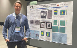
Jan O. Gaudestad presented the Poster “A new optical metrology technique for measuring the shape of a lithography photomask”
MADRID- 29th.02.24 SPIE Advanced Lithography and Patterning Conference, taking place between February 25th and February 28th in San Jose (California), took the attention from the entire semiconductor lithography and metrology industry. Its lineup of speakers were world-class leaders such as Anne Kelleher from Intel Corp, Todd Younkin from Semiconductor Research Corporation, and Chan Hwang from Samsung.
As part of this significant event, Wooptix will present a poster titled “New optical metrology technique for measuring the shape of a lithography photomask.” The presentation took place on the 28th at 5:30 PM in the Convention Center, Hall 2.
Jan O. Gaudestad, VP Business Development Manager, states: “Wafer overlay errors due to non-flatness and thickness variations of a mask need to be minimized to achieve good on-product overlay (OPO). Due to the impact on overlay errors inherent in all reflective lithography systems, EUV reticles will need to adhere to flatness specifications below 10nm, values which are nearly impossible to meet using current tooling infrastructure with current state-of-the-art reticles reporting Peak-to-Valley (PV) flatness of around 60nm².”
Jan O. Gaudestad, VP Business Development Manager
Through Wooptix’ poster, “We introduce a new technique, called Wave Front Phase Imaging (WFPI), that will generate a shape map with 810 thousand data points on an 86.4mm× 86.4mm area on an optical photomask with 96µm spatial resolution with a total data acquisition time of 14 seconds,” Gaudestad emphasizes.
The team involved in the paper includes Guillermo Castro, Miguel Jiménez, Kiril Ivanov, Juan M. Trujillo, José Manuel Rodríguez Ramos, and Jan Olaf Gaudestad, who was also the presenter that day.
Jan O. Gaudestad is based in San Francisco, US, and is responsible of the VP of Business Development for Wooptix. Before Wooptix, he was Director of BD at a VR startup and prior he worked on strategic accounts for motion sensors at InvenSense/TDK. He spent 14 years at Neocera, a backend semiconductor equipment maker where he was part of the team raising $13 million in 2002 to commercialize his graduate research work.
SPIE Advance Lithography and Patterning
SPIE Advance Lithography and Patterning took place in San Jose McEnery Convention Center, San Jose, California, from 25th to 29th and it hosted:
Additionally, it was possible to attend courses at Advanced Lithography + Patterning. “SPIE courses are designed to expand your knowledge and skills. Take what you learn in class and apply it directly to your work” says the organization.

An instructor during a training course at SPIE Advanced Lithography and Patterning Conference
You can get more info about the courses Here.
In the event was also possible to download the congress app. The SPIE´s web page explained “The app is free, easy to use, and loaded with features designed for planning and connecting on the go” The app can be downloaded Here
About SPIE
SPIE is the international society for optics and photonics. We strengthen the global optics and photonics community through conferences, publications, and professional development, bringing together engineers, scientists, students, and industry leaders to advance light-based science and technologies.
Inspired by the transformative power of photonics to enhance life around the globe, over the past five years SPIE has contributed more than $22 million to the international optics community.
About Wooptix
Wooptix is a leader in semiconductor metrology using wave front phase imaging, a technique derived from adaptive optics research in astronomy. With a multidisciplinary team, Wooptix aims to revolutionize the semiconductor metrology industry with the highest lateral resolution and fastest measurement technique for online factory measurements.
The company has developed Phemet®, a silicon wafer measurement tool, which is the precursor to the next fully automated manufacturing tool expected in 2024. Wooptix has already implemented Phemet® at various customer sites worldwide.
Wooptix is headquartered in Tenerife, Madrid (Spain), and San Francisco (USA).