


Miguel Jiménez, Kiril Ivanov Kurtev, Juan M. Trujillo-Sevilla, Rubén Abrante, Jose Manuel Ramos-Rodríguez, Jan O. Gaudestad
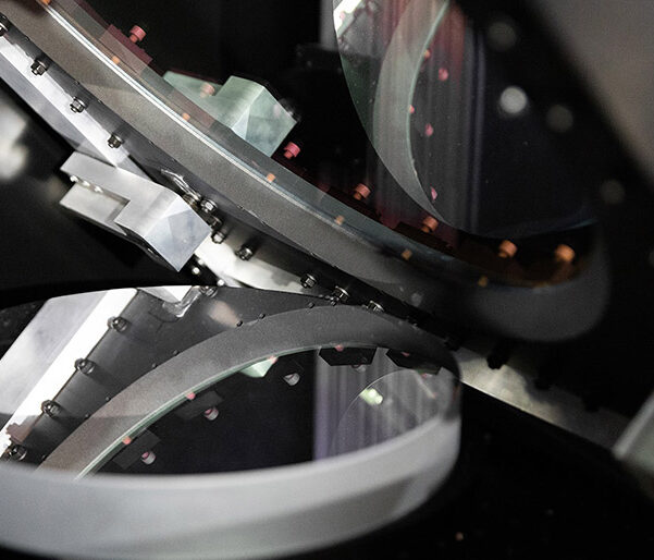
Wave Front Phase Imaging (WFPI), a new wafer geometry technique, is presented, that acquires 16.3 million data points in 12 seconds on a full 300mm wafer, providing lateral resolution of 65μm while holding the wafer vertically. The flatness of the silicon wafers used to manufacture integrated circuits (IC) is controlled to tight tolerances to help ensure that the full wafer is sufficiently flat for lithographic processing. Advanced lithographic patterning processes require a detailed map of the free, non-gravitational wafer shape to avoid overlay errors caused by depth-of-focus issues. For a wafer shape system to perform in a high-volume manufacturing environment, repeatability is a critical measure that needs to be tested. We present WFPI as a…