


Guillermo Castro, Kiril Ivanov, Miguel Jiménez,Juan M. Trujillo-Sevilla, Juan Manuel Ramos-Rodríguez, Jan O. Gaudestad.
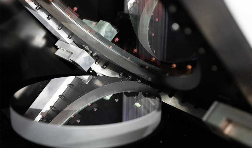
Wafer overlay errors due to non-flatness and thickness variations of a mask need to be minimized to achieve a very accurate on-product-overlay (OPO). Due to the impact of overlay errors inherent in all reflective lithography systems, EUV reticles will need…
Juan M. Trujillo-Sevilla, Rubén Abrante, Miguel Jímenez, Kiril Ivanov Kurtev, Guillermo Castro Luis, Jan O. Gaudestad
The shrinking depth of focus of high numerical aperture immersion microlithography optics requires a tight wafer flatness budget. Bare wafer surface topography variation is a significant part of the focus budget for microlithography. Thus, as the wafer surface quality becomes increasingly important, the metrology to control the surface quality is increasingly challenged1. Advanced lithographic patterning processes require a detailed map of the free, non-gravitational, wafer shape, to avoid overlay errors caused by depth-of-focus issues…
Juan M. Trujillo-Sevilla, Óscar Casanova-González, Alex Roqué-Velasco, Miguel Jesús Sicilia, Javier González Pardo, José Manuel Ramos-Rodríguez, Jan O. Gaudestad
On product overlay (OPO) is one of the most critical parameters for the continued scaling according to Moore’s law. Without good overlay between the mask and the silicon wafer inside the lithography tool, yield will suffer1. As the OPO budget shrinks, non-lithography process induced stress causing in plane distortions (IPD) becomes a more dominant contributor to the shrinking overlay budget2. To estimate the process induced in-plane wafer distortion after cucking…
Juan M. Trujillo-Sevilla, Alex Roqué-Velasco, Miguel Jesús Sicilia, Óscar Casanova-González, José Manuel Rodríguez-Ramos, Jan O. Gaudestad
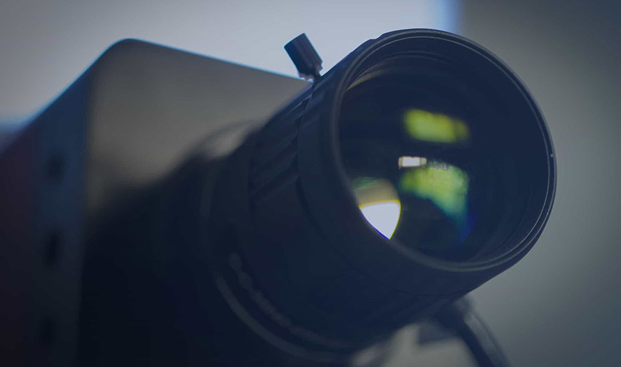
Wave Front Phase Imaging (WFPI) is a new wafer shape measurement technique that acquires millions of data points in just seconds or less, on a full 300mm silicon wafer. This provides lateral resolution well below 100μm with the possibility of reaching the lens’ optical resolution limitation between 3-4μm…
Ricardo Oliva-García, Sabato Ceruso, José G. Marichal-Hernández and José M. Rodriguez-Ramos
This work introduces a real-time full-resolution depth estimation device, which allows integral displays to be fed with a real-time light-field. The core principle of the technique is a high-speed focal stack acquisition method combined with an efficient implementation of the depth estimation algorithm, …
Juan Trujillo, Álvaro Pérez, Óscar Casanova, Miriam Velasco, Sabato Ceruso, Ricardo Oliva, Óscar Gómez, Javier Martín, Alex Roqué, José Manuel Rodríguez, Jan O. Gaudestad
Wave Front Phase Imaging (WFPI), a new wafer geometry technique, is presented, that acquires 7.65 million data points in 5 seconds on a full 300mm wafer providing lateral resolution of 96µm.
Wooptix’ team with the collaboration of Damien Gatinel & Jack T. Holladay
In this work, we characterize the in vivo ocular optics of the human eye with a lateral resolution of 8.6 microns, which implies roughly 1 million measurement points for a pupil diameter of 9 mm. The results suggest that the normal human eye presents a series of hitherto unknown optical patterns. This discovery could have a great impact on the way we understand some fundamental mechanisms of human vision.
Juan M. Trujillo-Sevilla, Oscar Casanova-González, Miriam Velasco-Ocaña, Sabato Ceruso, Ricardo Oliva-García, Óscar Gómez-Cárdenes, Javier Martín-Hernández, Alex Roqué-Velasco, Alvaro Pérez-García, José Manuel Rodríguez-Ramos, Jan O. Gaudestad
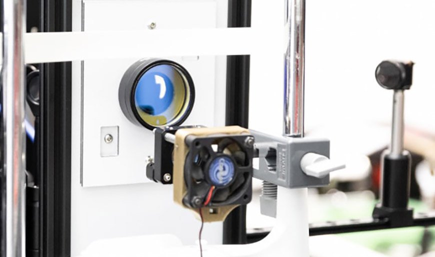
Wave Front Phase Imaging (WFPI) is used to measure the stria on an artificial, transparent plate made of Schott N-BK7® glass material by accurately measuring the Optical Path Difference (OPD) map. WFPI is a new technique capable of reconstructing an accurate high resolution wave front phase map by capturing two intensity images at different propagation distances. An incoherent light source generated by a light emitting diode (LED) is collimated and transmitted through the sample…
Álvaro Pérez-García, Juan M. Trujillo-Sevilla, Óscar Casanova-González, Miriam Velasco- Ocaña, Sabato Ceruso, Ricardo Oliva-García, Óscar Gómez-Cárdenes, Javier Martín-Hernández, Alex Roqué-Velasco, Álvaro Pérez-García, Jose Manuel Ramos-Rodríguez, Jan O. Gaudestad
The flatness of the silicon wafers used to manufacture integrated circuits (IC) is controlled to tight tolerances to help ensure that the full wafer is sufficiently flat for lithographic processing. Advanced lithographic patterning processes require a detailed map of the wafer shape to avoid overlay errors caused by depth-of-focus issues1. A large variety of new materials are being introduced in Back-End of Lines (BEOL) to ensure innovative architecture for new applications. The standard in-line control plan for the BEOL layer deposition steps is based on film thickness and global stress measurements which can be performed on blanket wafers to check the process equipment performance. However, the challenge remains to ensure high performance…
Sabato Ceruso, Sergio Bonaque-González, Ricardo Oliva-García, José Manuel Rodríguez-Ramos
The problem of reconstructing a depth map from a sequence of differently focused images (focal stack) is called Depth from focus. The core idea of this method is to analyze the sharpness of each pixel and compare it along the axis of the focal stack to estimate the true depth value. This approach has two main drawbacks: it depends on the optics of the camera and on the focus measure operator…