


Wooptix: Latest solution for on-product overlay
for wafer-to-wafer bonding processes
Wooptix, with its advanced silicon wafer shape measurement technique, is set to be an important contributor to the future of Semiconductor Advanced Packaging
To accomplish the challenging task of accurately overlaying two wafers during the hybrid wafer-to-wafer bonding process, an accurate wafer shape map is required.
At Semicon Europa (https://www.semiconeuropa.org/), Wooptix will present at the Advanced Packaging Conference (APC) (https://www.semiconeuropa.org/APC), its latest solution for on-product overlay for wafer-to-wafer bonding processes.
It will take place in November 15, held in the ICM (Internationales Congress Center München) adjacent to the Semicon Europa exhibition show.
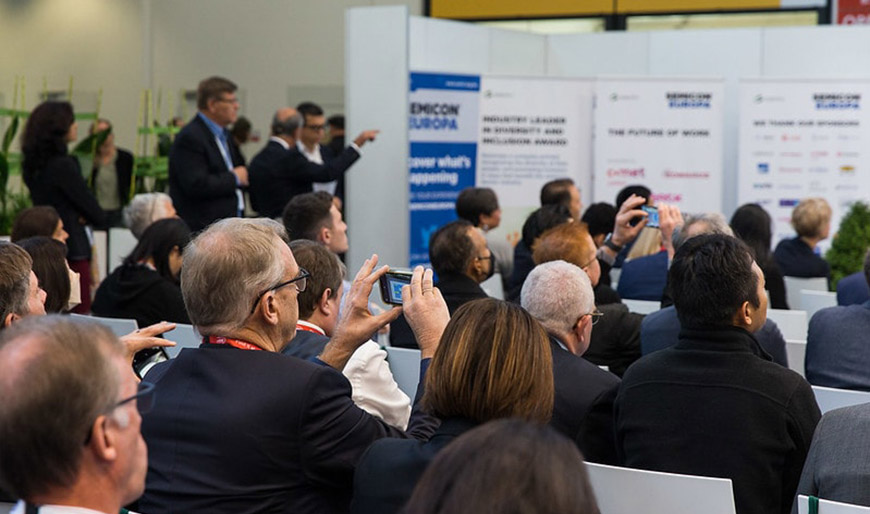
Semicon Europa
SEMICON Europa 2023 is co-located with productronica in Munich, Germany creating the strongest single event for electronics manufacturing in Europe and broadening the range of attendees across the electronics chain:
• Top-notch Keynotes
• Market Trends
• Exhibition
• Networking
• Advanced Packaging Forum / Fab Management Forum
• Smart Manufacturing / Mobility / MedTech
• Workforce Development and many more!
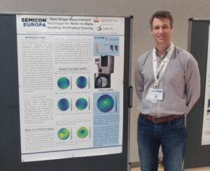
Wooptix Poster
Wooptix will present its poster in the Advanced Packaging Conference (APC), which will take place the Wednesday, November 15, from 9:00 am to 6:45 pm.
The webpage says: “This decade is expected to mark the $1T milestone for the semiconductor industry, driven by the latest trends in electrification and renewable energy, connectivity, and AI. This path will put the whole network under immense pressure including the supply chain, manufacturing plants, the energy sector, resources, and the environment to name a few. The industry will be relying on breakthroughs in innovation to sustain this growth. Heterogeneous integration, chiplets, fan-out wafer level packaging, and back-side metal depositions are all key development areas for advanced packaging and its industrial adoption, particularly for power application-centric areas such as the automotive industry”.
“Additionally, hybrid bonding, 3D stacking, and design-focused partitioning remain key to the continued extension of Moore’s Law. Testing and reliability continue to increase in focus for these multi-die solutions, giving rise to new requirements for data traceability across multiple manufacturing facilities”.
This year’s Advanced Packaging Conference (APC) will focus on:
• Megatrends and Opportunities for Advanced Packaging and Front-End Integration with a discussion about semiconductor advanced packaging Trends
• Smarter Supply Chain Solutions for a Sustainable Ecosystem and innovations in manufacturing equipment (e.g. for improved energy efficiency)
• Testing and Reliability: contacting challenges for non-standard and high-power packages and new reliability and test challenges imposed by new materials as well as the use of test data downstream and upstream to optimize manufacturing and packaging processes
• SiP Requirements for Future Applications with advanced packaging solutions for 5G and 6G designs, next-generation RF and power devices
• Power Electronics Packaging and current trends in electrification for industrial and automotive segments as well as the evolution from Si to SiC and GaN for power discrete and modules.
Register Now
You can still register Here
About Wooptix
Wooptix is a leader in semiconductor metrology through wavefront phase imaging, a technique derived from adaptive optics research in astronomy. With a multidisciplinary team, Wooptix aims to disrupt the semiconductor metrology industry with the highest lateral resolution and fastest measurement technique for inline fab measurements.
The company has developed Phemet®, a wafer shape lab tool for blank and patterned wafers, ahead of the upcoming fully automated fab tool, expected in 2024. Wooptix has already deployed Phemet® at several customer sites worldwide.
Wooptix is based at Tenerife, Madrid (Spain) and San Francisco (USA).