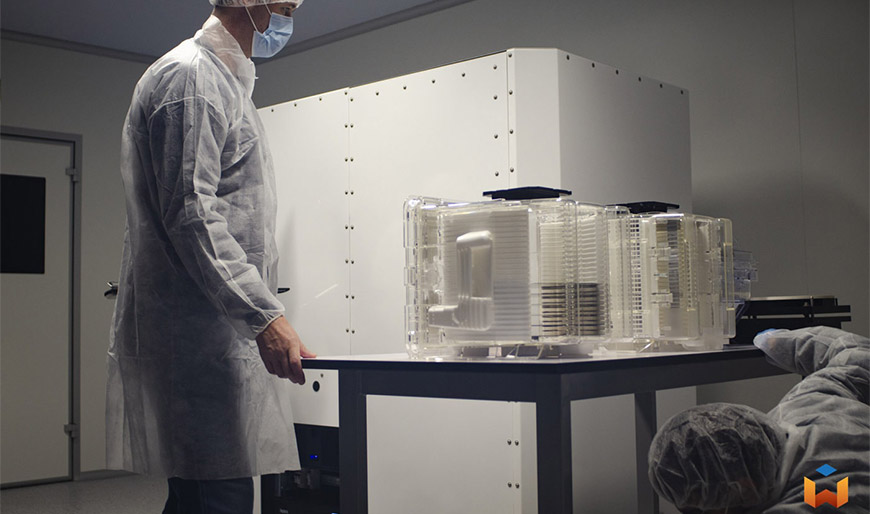
Wooptix expands its Clean Rooms and prepares 400 m² more to work in Semiconductor Metrology.
The clean rooms, which are located in the Nanotec building, in La Laguna (Tenerife), are complementing the investment in infrastructure that the company began two years ago.
Wooptix has announced the successful progress in the development of its two new clean rooms, which will be fully operational in mid-September. “The goal is to have more laboratories with zero levels of contamination to finish manufacturing the two Phemet® that we are delivering this year, and to start manufacturing its superior version: Phemet® Automation, which can perform metrology of semiconductors without the intervention of a person” says José Manuel Ramos, CEO of the company.
Wooptix’s investment in clean rooms means multiplying the current space by four, reaching 500 m². At this moment the company has two rooms, one of 30 m² and the other of 70 m², and in August the planning begins to adapt another 400 m², in the same Nanotec building. At the moment the clean rooms are being monitored by the team, looking for the suitability that allows them to work in accordance with the ISO14644-1 standard. “The weather conditions of the last few weeks are exceptional, with high temperatures and low humidity (normal average values are 20 degrees and 70% hum)” points out Javier Elizalde COO of Wooptix
Investment Closing Round B
It is relevant that Wooptix has closed a Round B investment of €10M in July and has been recognized with an EIC Accelerator Program, and with a €2.5M grant.
Current investors participated in round B: Bullnet Capital and CDTI (Centro para el Desarrollo Tecnológico Industrial) and Intel Capital, and it has been backed by new investors such as: Danobatgroup, Fagor Automation, Mondragón Promotion Fund and European Innovation Council Fund (EIC ).
More Clean Rooms – Next Steps
The Series B funding round represents the growth and consolidation of Wooptix. “It is very valuable for us to go from being an R&D company to being a product and manufacturing company. With this objective, we are generating all the necessary structures: from procedures and certifications, to protocols and work rooms with a low level of particles”, explains José Manuel Rodríguez Ramos.
“Automating Phemet® will reduce contamination of measured wafers and provide more reproducibility to the system. Without this breakthrough, it would not be possible to install these large systems in foundries. Due to the flexibility of our technique, the next step is the integration of Phemet® into existing semiconductor equipment” concludes Javier Elizalde.
About Wooptix
Wooptix is a leader in semiconductor metrology through wavefront phase imaging, a technique derived from adaptive optics research in astronomy. With a multidisciplinary team, Wooptix aims to disrupt the semiconductor metrology industry with the highest lateral resolution and fastest measurement technique for inline fab measurements.
The company has developed Phemet®, a wafer shape lab tool for blank and patterned wafers, ahead of the upcoming fully automated fab tool, expected in 2024. Wooptix has already deployed Phemet® at several customer sites worldwide.
Wooptix is based at Tenerife, Madrid (Spain) and San Francisco (USA).


