


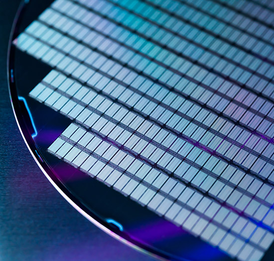
Patterned Wafer Geometry
// bonding On-Product Overlay
Shape Measurement
Shape Measurement
Technique for Wafer-to-Wafer
This new technique is available for wafer shape measurements of both single and bonded wafers. Knowledge of the shape can be used for finding voids and particles in between the two wafers.
Additionally, with advanced finite elements method (FEM) algorithms, one can calculate the predicted in plane distortions (IPD) for improved on product overlay (OPO), which is critical for successful hybrid bonding.
Are you interested in more information?
Please Fill this Form and we will keep in contact with you.
Ready to Get Started?
Your email address will not be published. Required fields are marked *