


Semiconductor Manufacturing
Phemet®
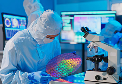
In the intricate field of semiconductor manufacturing, precision and reliability are crucial. Semiconductor devices demand an unprecedented level of accuracy in their production. As technology continues to advance, driving the constant miniaturization and complexity of these components, the role of metrology becomes increasingly decisive.
Semiconductor metrology encompasses a diverse array of techniques designed to scrutinize the physical, chemical, and electrical properties of semiconductor materials at various stages of the manufacturing process.
From the initial fabrication of wafers to the intricate assembly of integrated circuits, metrology serves as the discerning eye, ensuring that each component meets stringent quality standards
The Essential Role of Semiconductor Metrology in Technological Innovation
As manufacturers strive to push the boundaries of what is technologically achievable, semiconductor metrology emerges as an indispensable tool, providing the meticulous measurements essential to produce cutting-edge electronics.
Phemet® Technology
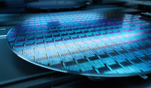
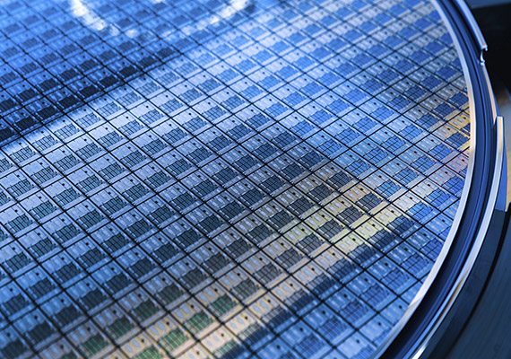
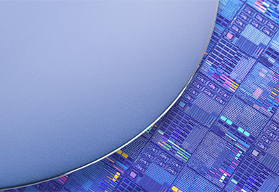
Wooptix WaveFront Phase Imaging (WFPI) is a new semiconductor wafer geometry technique that measures: (Of the entire silicon wafer in a non-contact, single image snapshot.)
Shape uniformity
Pedir texto
Nanotopography
Pedir texto
And roughness
Pedir texto
Collecting more than 10 million data points with sub-nanometer height resolution, WFPI is the industry leader in speed and resolution.
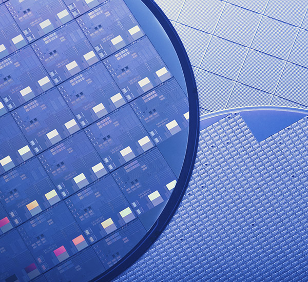
With the ability to measure both:
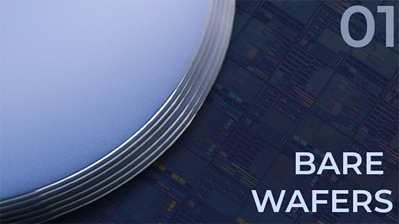
- Bare wafers
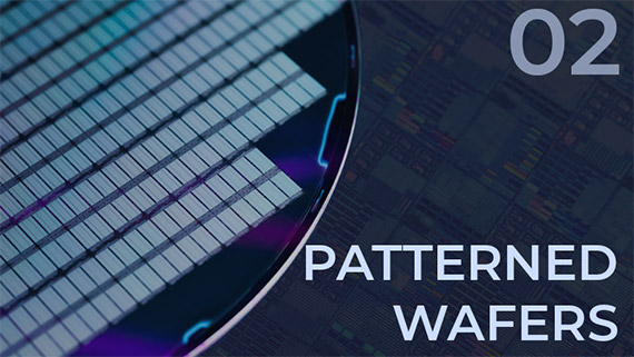
- And patterned wafers
The wafer manufacturer, as well as the semiconductor device maker, will take advantage of the speed and accuracy offered by our technology WFPI, used in Phemet®.
How Wooptix can help?
Through WFPI (Wavefront Phase Imaging)
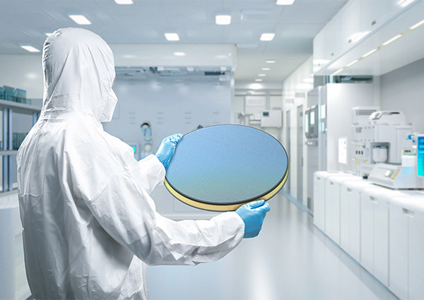
Wooptix has developed a system called Phemet®, that uses WFPI, a proprietary wavefront sensing technique.
Phemet® introduces a new semiconductor wafer geometry technique that measures: shape uniformity, nanotopography, and roughness of the entire silicon wafer in a single image. By collecting more than 10 million data points with subnanometer height resolution, Phemet® is the industry leader in speed and resolution.
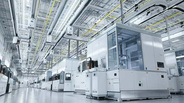
Wooptix's Metrology Systems Revolutionize and Process Control
Wooptix´s s systems for wafer inspection and metrology in advanced wafer-level packaging offer the essential data needed by chip manufacturers to enhance yield through comprehensive traceability in their progressively intricate manufacturing procedures.
The demand for tighter process control has intensified due to smaller feature sizes, novel integration approaches, and the diverse integration of multiple components into unified packages.
Wooptix Systems empower corporations to swiftly identify, address, and track deviations, ensuring heightened quality control for enhanced device performance
Same System to Measure
SEBI is a high-resolution light field camera capable of obtaining depth and color information in real time enabling live video.
PEDIR TÍTULO
PEDIR TÍTULO
WPFI applied to the Industry
The technique involves capturing and analysing the phase information of a wavefront, providing valuable insights into the characteristics of light or other waves.
Applied to Metrology, Wavefront phase imaging can be employed in material inspection to analyze the surface quality and characteristics of objects.
In metrology, it aids in the precise measurement of shapes and dimensions, contributing to quality control processes.

Wooptix WaveFront Phase Imaging (WFPI) is a new semiconductor wafer geometry technique that measures:
Collecting more than 10 million data points with sub-nanometer height resolution
- Bare wafers
- And patterned wafers


Lower Noise
Due to its fast acquisition, Wooptix System (Phemet®) emits less noise
Lower Noise
Besides and very important, due to no moving parts in the system when acquiring the wavefront phase of the wafers, WFPI has low noise. Instead of having to choose the right wafer geometry metrology solution for your products, choose the one system that can measure all types of samples with superior performance in the same system.
Due to its fast acquisition, Wooptix System emits less noise

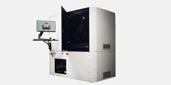
What is the System
Tool Concept
Wave Front Phase Imaging Phemet® is offered as a manually operated 200mm and 300mm wafer metrology tool.
The custom software allows the system to measure 200mm and 300mm wafers using different analysis windows.

Automatic Tool
The upcoming fully automated fab tool is expected in 2024. The use of the automatic tools will:
- Enhance efficiency
- Reduces human error
- Enable real-time monitoring
These tools play a pivotal role in maintaining the quality standards required for the production of reliable and high-performance semiconductor chips.
What is the System
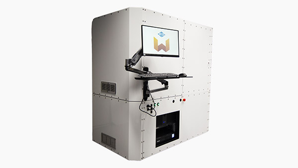
Tool Concept
Wave Front Phase Imaging Phemet® is offered as a manually operated 200mm and 300mm wafer metrology tool.
The custom software allows the system to measure 200mm and 300mm wafers using different analysis windows.
Automatic Tool
The upcoming fully automated fab tool is expected in 2024. The use of the automatic tools will:
- Enhance efficiency
- Reduces human error
- Enable real-time monitoring
These tools play a pivotal role in maintaining the quality standards required for the production of reliable and high-performance semiconductor chips.
Tool Concept
Wave Front Phase Imaging Phemet® is offered as a manually operated 200mm and 300mm wafer metrology tool.
The custom software allows the system to measure 200mm and 300mm wafers using different analysis windows.
Automatic Tool
- Enhance efficiency
- Reduces human error
- Enable real-time monitoring
What do we have
Phemet® has been evaluated by major semiconductor players in Europe, Asia and the US. Wooptix is working on the next fully automated and robotic manufacturing tool.
Phemet® Specifications
The main Phemet® Specs are available.
If you would like to download the Phemet Specs and Data sheet, please fill this form.