


WFPI is based on registering the intensity distribution at two different optical planes using two conventional imaging sensors while acquiring two images with the exact same field of view…
Poster exhibited at the Semicon Taiwan 2020.
JAN OLAF GAUDESTAD
VP Business Development
WFPI is based on registering the intensity distribution at two different optical planes using two conventional imaging sensors while acquiring two images with the exact same field of view.
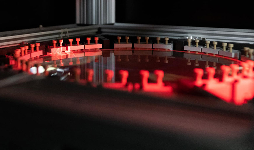
The wave front phase is translating into measuring the slope of the surface, which allows for a geometric reconstruction of the silicon wafer. WFPI system can be achieved by using a powerful LED to illuminate the silicon wafer through a bitelecentric lens and measuring the reflected intensity using 2 industrial cameras at different locations along the optical path.
An entire silicon wafer can be imaged in a single snap shot providing depth information in every pixel acquired.